
The Graphene-Info newsletter ( May 10, 2022 )
posted on
May 10, 2022 11:45AM

Hydrothermal Graphite Deposit Ammenable for Commercial Graphene Applications

Cannot read this? View it online here
Japan's Ministry of Education, Culture, Sports, Science and Technology has launched a collaborative project to develop 2.5D materials. The project, titled "Science of 2.5 Dimensional Materials: Paradigm Shift of Materials Science Toward Future Social Innovation" includes 40 researchers in Japan, led by Prof. Ago Hiroki at Kyushu University.
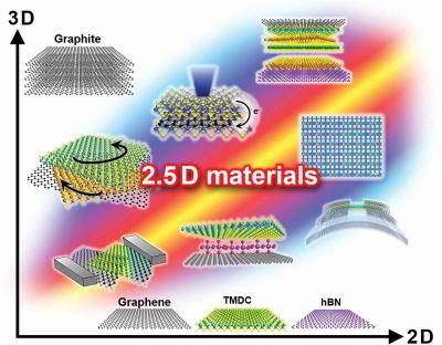
2.5D materials are made by stacking different 2D materials artificially by using advanced transfer techniques. These new materials are not limited by lattice constant or composition, and it is possible to control the material layers, and their stacking angle. These new materials could unlock new breakthroughs in materials science.
The 2D Experimental Pilot Line (2D-EPL), that originated from the Graphene Flagship, recently launched its first customizable wafer run.
As one of five multi-project wafer (MPW) runs, this first phase is targeting sensor applications. Companies, universities and research institutes can include their designs as dies on joint wafers, to test their ideas for devices on a larger scale at relatively low costs. The first 2D-EPL MPW run opened in February and the call closes on 30 June 2022. The manufacturing stage of the MPW run will take place between 1 September and 31 October 2022.
Researchers from the University of Maryland have explored the somewhat creative possibility that our reality is only one half of a pair of interacting worlds, drawing inspiration from bi-layer graphene. Their mathematical model may provide a new perspective for looking at fundamental features of reality—including why our universe expands the way it does and how that relates to the most miniscule lengths allowed in quantum mechanics.
The scientists formed this new perspective based on the study of bi-layer graphene. They realized that experiments on the electrical properties of stacked sheets of graphene produced results that looked like little universes and that the underlying phenomenon might generalize to other areas of physics. In stacks of graphene, new electrical behaviors arise from interactions between the individual sheets, so perhaps unique physics could similarly emerge from interacting layers elsewhere—perhaps in cosmological theories about the entire universe.
CAP-XX, Australia-based manufacturer of thin-form supercapacitors and energy management systems, recently formed a joint venture for what it calls a "transformational new graphene material".
The deal is with Australia's Ionic Industries, which is developing new forms of graphene for a variety of markets, and involves the commercialization of reduced graphene oxide (rGO) for supercapacitors and other energy storage devices.
NanoXplore and Solmax Group have announced that they have entered into a blanket purchase order, following several years of collaborative work.
The five-year collaboration between the two companies has reportedly resulted in a product and Solmax CEO, Jean-Louis Vangeluwe, said: “This cooperation underscores our commitment to delivering growth through forward-looking innovation and collaboration. Our five-year development collaboration with NanoXplore will allow us to launch a next-generation product based on graphene technology that solves some of our customers’ sustainability challenges while also boosting performance.”
University of Pennsylvania scientists have recently conducted a study that shows how patterned, periodic deformations of a single layer of graphene transforms it into a material with electronic properties previously seen in twisted graphene bilayers. This system also hosts additional unexpected and interesting conducting states at the boundary.
Through a better understanding of how unique properties occur when single sheets of graphene are subjected to periodic strain, this work has the potential to create quantum devices such as orbital magnets and superconductors in the future.
This is a sponsored post by Graphenea
Graphenea has announced that, following the release of its GFET S30, it has developed a High-K Metal Gate (HKMG) manufacturing process to create Field-Effect Transistor (FET) structures on graphene, or GFETs. This process is now available under the dedicated GFAB service, starting February 2022.
HKMG structures triggered a revolution in Si electronics when they were introduced during the early 2000’s, creating an alternative to SiO2 gate dielectrics that paved the way for further scaling. HKMG technology indeed enabled Moore’s law to continue, providing increased capacitance and lower current leakage than the previously state-of-the-art SiO2 tech. The most common FET architecture to modulate the conductance in graphene uses a SiO2 gate dielectric grown on top of a heavily doped Si substrate. Whereas this structure is easy to implement, it suffers from excessive current leakage when the SiO2 layer is thinned down, often rendering devices unusable. Moreover, the substrate acts as a global backgate, forbidding manipulation of individual GFET devices, which is essential for many applications.
Versarien has announced that its Graphene-Wear technology will be incorporated in gear to be used by players from West Ham United, Werder Bremen and England’s rugby union squad next year, as part of a new project with Umbro.
The technology will provide the players with “enhanced thermal transmittance, increased moisture management, with improved drying rate, without compromising air or water vapor permeability”.