Photonics Reshapes the Future of Computing Ayar Labs,Lighmatter, Lightelligence
posted on
Feb 21, 2024 09:48AM


https://www.photonics.com/Article.aspx?AID=69683
As Moore’s law approaches its limits, advancements in materials science, chip architectures, and quantum technology are opening new paths for electro-optics to enable faster, lower-power computers.
Moore’s law has been challenged many times during the past sixty years, but semiconductor engineers always found new tricks to continue doubling the density of transistors on a chip. In the meantime, the cost to do so has skyrocketed. Today, chip makers create structures on silicon chips that are as thin as a few atoms. It will not be long before physics prevents these structures from getting any smaller.
Decreasing the transistor size has always helped to increase the clock rate. There are other ways to enable higher processing speeds, such as cooling or using lower voltages. But most of these methods will also reach their physical limits in a few years, which will inhibit processors from getting faster.
At the same time, the demand for computing power continues to rise, not least due to the advent of artificial intelligence (AI). Furthermore, there is a well-founded demand to limit the power consumption of computer chips, even if the performance of computers or data centers does increase unabated.
Obviously, the problems with electronics amount to basic, physical-level issues, whereas the demand for computing power increases unabated.
Photonics offers potential solutions. We have all benefited from optical fibers replacing copper wires to enable much faster internet in our homes. Light waves have much higher frequencies compared to electronic signals, allowing for higher signal transmission rates. And light waves can be superposed. That is, signals of different wavelengths can be transmitted at the same time in the same fiber.
The ever-faster data transfer opportunities enabled by optoelectronic technology have reached an industrial scale. At the core of this technology are optical transceivers, devices able to both transmit and receive optical signals. Current off-the-shelf optical 400G transceivers transmit 400 Gb/s, and 800G transceivers are now reaching the market. It should be noted that the 400G devices exhibit 100× higher clock rates than the central processing units (CPUs) in a regular office computer.
Transceivers perform an essential role in today’s data centers, where the rate at which data can be transferred is crucial to performance. Currently, they largely connect servers to servers or racks to racks. As soon as a data signal reaches the circuit board within a server, the fiber advantage is lost and transmissions are made electronically. If photonic signals could be brought closer to the CPUs and graphics processing units (GPUs), then data centers would leverage gains in both speed and energy efficiency.
This is easier said than done, however. Photonic data links are much more difficult to manufacture and manage compared with conventional electrical lines.
Onboard optical connections mostly rely on waveguides, mirrors, and coupling schemes that are all alignment sensitive. Poorly aligned or coupled optical components induce signal loss, which makes integrated photonics difficult to package.
Integration of these components on a wafer often leverages traditional CMOS manufacturing processes from the semiconductor realm that have been adapted to the world of photonics. But silicon does not lase and, therefore, integrated photonics solutions require the introduction of unfamiliar materials, such as indium phosphide, silicon nitride, and lithium niobate to provide optical functions. Alternate substrate materials, such as glass, are also under consideration. Intel named Srinivas Pietambaram its 2023 Inventor of the Year for his research on glass as a substrate for computer chips. Glass carries the potential for a 10× increase in interconnect density and integration of optical interconnects. In its announcement about Pietambaram, Intel reported it is working internally and with foundry customers to plan the first products built with a body of glass.
Optical I/O chips off the shelf
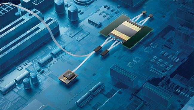
The difficulties in efficiently bringing optical signals to the board and chip level have so far limited the commercial applications for such architectures. But that is beginning to change. Ayar Labs, a startup based in Silicon Valley, has developed its TeraPHY chiplet for in-package optical input/output (I/O) and is producing it in GlobalFoundries’ high-volume 45-nm fabrication process. In a white paper published by Ayar Labs, the company reports that its chiplet “integrates millions of transistors with hundreds of photonic devices to drive tens of Tbps [terabytes per second] of bandwidth up to 2 km out of the package with unmatched power efficiency of less than 5pJ/b1.” Figure 1 shows an example of how such optical I/O chiplets can be packaged with electronic chips.
Figure 1. A representative example of how four optical input/output (I/O) chiplets might be integrated into a package with a system-on-a-chip solution. The package connection relies on fiber ribbon arrays. Courtesy of Ayar Labs.
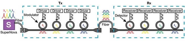
Ayar Labs separated the actual light source, which consists of heat-sensitive laser diodes, from the I/O chiplet and its neighboring heat-producing systems-on-chips (SoCs) (Figure 2).
Figure 2. A schematic of Ayar Lab’s multiwavelength SuperNova remote light source attached to the company’s TeraPHY optical input/output (I/O) chiplet (Tx), which sends its signals through a fiber to a receiving I/O chiplet (Rx). Courtesy of Ayar Labs.
The light source, capable of emitting up to 16 wavelengths, is capable of supplying light for 256 channels with a bidirectional bandwidth capacity of 4 Tbps. It is about the size of a smartphone SIM card.
In autumn 2023, Ayar Labs presented its latest innovation, an optical field- programmable gate array (FPGA) consisting of two of the company’s optical I/O chiplets connected to a 10-nm FPGA fabric die, the core fabric used in Intel’s Agilex FPGAs. Two SuperNova light sources power the device’s optical com- munication and support 64 optical channels across eight fibers on each chiplet. Ayar claims its configuration can deliver 5× more bandwidth at a fraction of the power (<5pJ/b) and latency (5 ns per chiplet + time of flight), positioning it as a potential future solution for data-intensive applications, such as generative AI, machine learning, and novel disaggregated computer and memory architectures.
(full article continues at link)